产品与技术
Products and Technology
List of Semiconductor Products
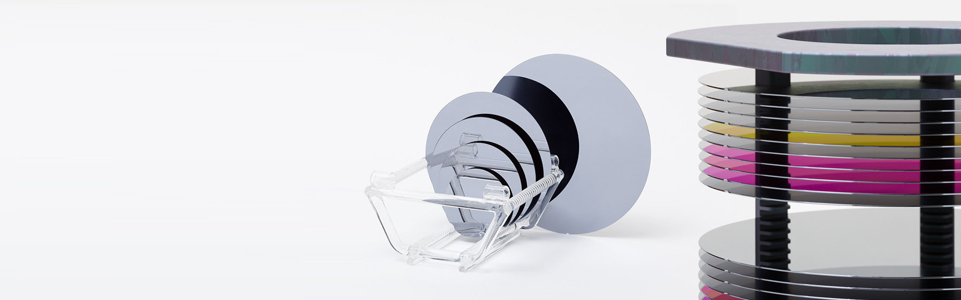
Single Crystal Ingot

We use the CZochralski method (Czochralski) to grow P-type and N-type dislocation-free silicon ingots with crystal orientations of <100>, <111> or <110> respectively. Through high-purity quartz crucibles, superconducting magnetic fields and other applications, we provide Low COP, COP Free, low metal content and high-quality, 100mm/125mm/150mm/200mm/300mm silicon single crystal ingots.

Polished Wafer
Polished Wafer

The single crystal ingot is prepared after the processes of slicing, lapping, etching, DK , CVD, polishing, etc., to obtain a polished wafer with high flatness, excellent geometric parameters, clean surface and mirror-like state.


Epitaxial Wafer
Epitaxial Wafer

By orderly growing a layer of monocrystalline silicon on a silicon substrate, an epitaxial wafer with a target resistivity thickness is prepared, thereby obtaining a high-quality silicon wafer to meet the requirements of preparing a device.


Anneal Wafer
Anneal Wafer

After the silicon wafer is annealed at a high temperature in an argon annealing furnace, the interstitial oxygen in the near surface area of the silicon wafer is diffused outward, thereby eliminating the void-type micro-defects in the near surface area, forming a clean area, which can improve The electrical properties of silicon wafers.


XML 地图